BITS Pilani and Siemens EDA launch joint PCB design certification
BITS Pilani and Siemens EDA have partnered to launch joint certification programmes in PCB design and analysis. Offered through WILP centres, the courses aim to train students and professionals with practical skills for the electronics and semiconductor industry
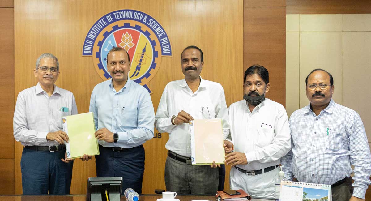
Hyderabad: BITS Pilani, through its Work Integrated Learning Programmes (WILP), and Siemens EDA have announced a collaboration to launch joint certification programmes in PCB Design and Analysis, aimed at strengthening the electronics and semiconductor talent ecosystem in the country.
The programme is designed to develop industry-ready professionals with hands-on expertise in schematic and multilayer PCB design, high-speed signal integrity, power integrity and EMI/EMC analysis. Participants will train on Siemens EDA’s Xpedition and HyperLynx platforms, gaining practical skills aligned with real-world design and manufacturing needs.
Delivered through BITS Pilani WILP’s Smart Manufacturing Competency Centres, the joint certification will focus on experiential and problem-based learning. The programme will be open to working professionals, students and industry engineers, addressing critical skill needs across semiconductor design, automotive electronics and industrial automation.
Siemens EDA Vice President and Country Manager Ruchir Dixit said the programme aims to create a strong pipeline of future-ready engineers, equipped with application-driven skills and industry-leading tools, to support India’s design-to-manufacturing innovation goals.
BITS Pilani Group Vice Chancellor Prof. V Ramgopal Rao said, “By bringing cutting-edge tools and industry practices directly into the hands of our learners, we are helping them build the confidence and skills needed to contribute meaningfully to India’s semiconductor and electronics journey.”